


SRAM vs. DRAM: Which one is better?
September 15 2023 
Inquiry
Global electronic component supplier AMPHEO PTY LTD: Rich inventory for one-stop shopping. Inquire easily, and receive fast, customized solutions and quotes.
QUICK RFQ
ADD TO RFQ LIST
SRAM, or static RAM, offers better performance than DRAM since it doesn't need to be refreshed as often while it's in use. SRAM is less dense and more expensive while having sizes that are orders of magnitude less than DRAM.
What is SRAM?
Random access memory comes in the form of static random-access memory (SRAM). The word "static" describes how the information kept in this kind of memory doesn't change as long as it's powered on. In contrast, Dynamic Random Access Memory (DRAM) data needs to be updated on a regular basis. In contrast to ROM or flash memory, which may continue to store data even after a power outage, data saved in SRAM is called volatile memory since it disappears when the power supply fails.
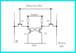
The basic structure of SRAM
Static Random Access Memory (SRAM) includes two essential features. Data is kept in a static format: This means that the data is saved in the semiconductor memory and does not require refreshing as long as the memory is powered on. Random-access memory comes in the form of SRAM memory: Regardless of the sequence in which the previous memory location was accessed, random-access memory can write or read places in semiconductor memory. A single SRAM memory cell's circuitry normally consists of four transistors that have been set up as two cross-coupled inverters. The circuit has two stable states in this configuration, which are the logic "0" and "1" states. Since bipolar transistor technology—another viable option—consumes substantially more power than MOS circuits, the transistors are MOSFETs.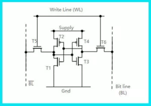
What is DRAM?
Dynamic Random Access Memory, or DRAM, has become the standard type of memory. A transistor and a capacitor with a charge that represents "1" and no charge that represents "0" make up the fundamental component. Random Access means that the time it takes to read or rewrite any of these bits is the same because the charge in the capacitor seeps out slowly over time and must be "recharged" at regular intervals, which is how the term "Dynamic" came to be used. Reading or rewriting any of these bits requires the same amount of time due to random access. Due to its low cost, fast access speed, and straightforward design, which makes large-scale integration possible, DRAM is now widely used. The DRAM hierarchy is roughly divided into channel, rank, DRAM chip, bank, memory array, and memory cell, with the memory cell serving as the most fundamental storage unit and having storage objects of 1 or 0. The bank is the smallest controllable unit. The rank is roughly equivalent to a "memory stick." "memory stick" (a memory stick can contain many ranks), and the number of channels roughly equates to the number of memory sticks.
The basic structure of DRAM
The lower static power is the six-transistor SRAM circuit's key benefit. The pull-down resistors in the four-transistor variant always have current flowing through them, which raises the chip's overall power consumption. This may limit the degree of integration and make circuit design issues worse because of higher power dissipation. The four-transistor SRAM computer memory cell offers certain benefits in terms of density, but this comes at the expense of manufacturing complexity since resistors must be produced, which necessitates additional processing. The resistors must also be small in size and have high resistance values in order to meet the demands of the cell. For instance, a standard three-transistor DRAM cell (see above) carries out a write command by applying a voltage to the gate of the M1 access transistor, which then charges the gate capacitor of the M3 transistor. The charge held in the M3 gate capacitor steadily dissipates as the write line is then driven down; this process is known as dynamics.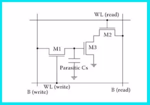
How does an SRAM work?
An SRAM cell typically has 4-6 transistors, and when it is given a state of 0 or 1, it will hold that state until it receives a new state or until there is a power outage, at which point it will change or disappear. SRAM is reasonably quick and power-efficient, but it requires 4-6 transistors to store 1 bit of information, which increases the cost of production. In contrast, DRAM can be produced with just one transistor. Two CMOS inverters make up the basic SRAM cell, and their inputs and outputs are cross-connected, meaning that the output of one inverter is connected to the input of another, while the output of another inverter is connected to the input of the first. This makes it possible to lock and save the output states of the two inverters, or to store the state of one bit. In general, a basic cell's footprint will be smaller the fewer transistors there are inside of it. Since the cost of manufacturing silicon wafers is comparatively fixed, the cost of each bit of storage decreases as the size of the SRAM basic cell decreases, allowing for more bit storage to be produced on the chip. The write 0 and write 1 operations serve as an introduction to the comparatively straightforward workings of SRAM.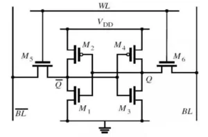
Write 0 operation:
First, enter level 0 into BL and level 1 into (BL) to write 0. M5 and M6 will then turn on after the corresponding Word Line (WL) has been selected. The G-pole control terminals of M1 and M2 receive input at level 0, while M3 and M4 get input at level 1. M2 has a high-level cutoff and a low-level turn-on because it is a P-type tube. M1 is the opposite, having low-level cutoff and high-level conduction. A level of 0 will cause M1 to stop and M2 to start. At a high level, the (Q) point will be stable. Similar to this, high levels will be sent to the control terminals of M3 and M4, and because of their distinct NP tubes, M3 will conduct and M4 will switch off. The Q point will level off at a value of 0. The internal M1, M2, M3, and M4 will then be in a stable condition, and a bit 0 of data will be latched. At this point, M5 and M6 will be switched off. This content will continue without turning on the external VDD at this time.Write 1 operation:
The read procedure is rather straightforward; all that is required is to precharge BL and (BL) to a specific high level, turn on M5 and M6, and then use the differential amplifier to read out the latched contents.How does a DRAM work?
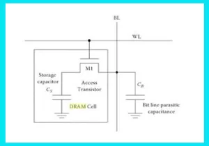
Transistors and tiny capacitance-f capacitor storage cells make up DRAM. A tiny etched transistor is built into each memory cell and is kept in storage, or turned on and off, by the charge of a tiny capacitor. The capacitor has features in common with a tiny rechargeable battery. It can be electrically charged to represent a 1 and discharged to represent a 0, respectively. Charged capacitors must constantly be "refreshed" with a new charge because they lose their charge when discharged.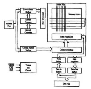
SRAM/DRAM Advantages and Disadvantages Comparison
| Pros of SRAM: |
| There is no need to set up separate circuits for routine refreshes because latches memorize data. |
| Fast access times (SRAM is built using the same semiconductor technology as CPUs). |
| Cons of SRAM: |
| Compared to DRAMs, all components are more numerous and less integrated. |
| Increased electricity usage. |
| Larger size, more expensive to manufacture than DRAM. |
| Pros of DRAM: |
| The peripheral circuit requires more frequent refreshing and is more complicated. |
| Refreshing devices are not capable of reading or writing, which limits their ability to use time efficiently. |
| Cons of DRAM: |
| Centralized refresh: During a predetermined refresh cycle, all storage units are brought together for a period of time to undergo a gradual refresh; during this time, reading and writing operations must cease. |
| Decentralized refresh: Each row of storage units undergoes a distributed refresh that is finished throughout each storage cycle. |
| Combining centralized and decentralized refresh, asynchronous refresh. |
SRAM vs. DRAM
| SRAM | DRAM |
| High-performance applications employ SRAM. | DRAM is utilized in all kinds of applications. |
| High-speed cache memory using SRAM. | DRAM is a component of slower main memory. |
| Information is stored in SRAM as long as power is available. | DRAM retains information for a brief period of time after the power is turned off or as long as the electricity is supplied. |
| In SRAM, information is stored using transistors. | In DRAM, capacitors are utilized to store data. |
| Compared to DRAM, SRAMs are more radiation-resistant. | Compared to SRAMs, DRAMs are less radiation-resistant. |
| There is no requirement for refreshing because there are no capacitors used. | The capacitor's contents must be updated on a regular basis in order to preserve information for a longer amount of time. |
| less heat is produced and less power is consumed. | more heat is produced and more power is consumed. |
| Bits are stored in this as voltage. | Electric energy is used to store the bits in this. |
| Low-density devices include SRAMs. | Devices with a high density are DRAMs. |
| SRAM is quicker than DRAM. | DRAM offers sluggish access rates. |
Differences between SRAM and DRAM
SRAM, or static RAM, provides higher performance than DRAM since SRAM does not require regular refreshment while DRAM does when it is in operation. Despite having sizes that are orders of magnitude smaller than DRAM, SRAM is less dense and more expensive. SRAM and DRAM are primarily distinguished by the fact that SRAM is an on-chip memory type with a quick access time while DRAM is an off-chip memory with a slow access time. SRAM operates better than DRAM as a result. The data is stored in SRAM using transistors. In DRAM, capacitors are used to store the data, while the data is stored in SRAM using transistors. In DRAM, capacitors are used to store the data. In terms of speed and price, SRAM performs better than DRAM. Compared to SRAM, DRAM offers larger storage space. Cache memory uses SRAMs, whereas main memory uses DRAMs.SRAM vs. DRAM FAQ
What are the main differences between SRAM and DRAM?
SRAM and DRAM are the two varieties of RAM. The fundamental distinction between SRAM and DRAM is that SRAM is an energy-efficient memory chip type that is faster than DRAM. DRAM, on the other hand, is a memory chip that uses more power but can store more data than SRAM.SRAM vs. DRAM: Which one is better?
Since SRAM, also known as static RAM, does not need to be refreshed on a regular basis while DRAM does while it is in use, SRAM offers better performance than DRAM. SRAM is more expensive and less dense than DRAM while having sizes that are orders of magnitude less.What is the primary drawback of utilizing DRAM instead of SRAM?
All storage units of DRAM are brought together for a period of time to undergo a gradual refresh during a predetermined refresh cycle; reading and writing operations must stop during this time. Distributed refreshes are completed for each row of storage units throughout each storage cycle.Drawbacks or disadvantages of SRAM
SRAM has a bigger size and is more expensive to produce than DRAM. Its components are also more numerous and poorly integrated.What is DRAM?
Dynamic random access memory (DRAM), a form of semiconductor memory, is frequently used to store the data or program code needed for a computer processor to operate. DRAM is a popular variety of random access memory (RAM) that is utilized in servers, workstations, and personal computers (PCs).What is the size of SRAM and DRAM?
SRAM has a storage capacity of 1MB to 16MB, but the common DRAM sizes in laptops and smartphones are 4 to 16GB and 1GB to 2GB, respectively.Related Articles
Populer Posts