


SAR ADC-A Specific Type of ADC
September 08 2023 
Inquiry
Global electronic component supplier AMPHEO PTY LTD: Rich inventory for one-stop shopping. Inquire easily, and receive fast, customized solutions and quotes.
QUICK RFQ
ADD TO RFQ LIST
A Successive Approximation Register (SAR) ADC is a type of analog-to-digital converter that uses a binary search algorithm to convert analog signals into digital form. Gain insights into the working principles, advantages, and disadvantages of this converter.
What is SAR ADC?
A SAR ADC, or Successive Approximation Register Analog-to-Digital Converter, is a type of analog-to-digital converter commonly used in electronic devices to convert analog signals into digital data. The SAR ADC operates by using a binary search algorithm to approximate the digital value of an input analog signal. It is known for its high resolution, speed, and accuracy. The main advantages of SAR ADC are low power consumption, small size, high precision, moderate resolution and speed, and short sampling delay. It is an economical ADC implementation, so it is widely used in MCU/SOC.What is the Difference between ADC and SAR ADC?
An ADC, or Analog-to-Digital Converter, is a broad term used to describe any device or circuit that converts an analog signal into a digital representation. On the other hand, a SAR ADC, or Successive Approximation Register Analog-to-Digital Converter, is a specific type of ADC with a unique architecture and operating principle. The main difference between an ADC and a SAR ADC lies in their working principles and conversion methods. Below is a chart for understanding.|
Aspect |
ADC | SAR ADC |
|
Conversion Method |
Various methods (e.g., Delta-Sigma, Flash) | Successive Approximation |
|
Resolution |
Variable (typically 8-24 bits) | Variable (typically 8-18 bits) |
|
Speed |
Varies (can be fast or slow) | Moderate to high-speed |
|
Complexity |
Can be complex | Relatively simple |
|
External Components |
May require external components | Minimal external components required |
|
Power Consumption |
Varies (can be high or low) | Low power consumption |
|
Accuracy |
High accuracy in some types | Good accuracy and linearity |
|
Sampling Rate |
Variable (depends on the type) | Limited by the speed and resolution |
|
Applications |
Wide range of applications | Suitable for many applications |
|
Cost |
Varies (can be low or high) | Generally cost-effective |
How to Design SAR ADC?
Designing a SAR (Successive Approximation Register) ADC (Analog-to-Digital Converter) involves several key steps. Here, we will outline a general process for designing a SAR ADC:Define Specifications
Determine the required resolution: Decide on the number of bits needed for the digital output based on the desired accuracy. Establish the sampling rate: Determine the rate at which the ADC will sample and convert the analog input signal. Consider other requirements: Take into account factors such as power consumption, input voltage range, and tolerable error.Determine Architecture
SAR ADC architecture consists of a comparator, a DAC (Digital-to-Analog Converter), and a control logic block. Select the appropriate comparator: Consider factors like speed, power consumption, and noise performance. Choose the DAC type: Common choices include binary-weighted capacitor arrays or segmented DACs. Design the control logic: Develop the logic circuit that controls the conversion process.Select Components
Choose suitable components based on the determined architecture and specifications. Select operational amplifiers for the comparator and any required buffers. Determine the type and size of capacitors for the DAC, considering linearity and settling time requirements. Identify suitable digital logic components for the control logic block.Circuit Design
Design the analog circuitry, including the comparator, DAC, and any necessary amplifiers or buffers. Use appropriate techniques to minimize noise, optimize linearity, and maximize performance. Implement the control logic circuitry, which generates the digital control signals for the conversion process.Layout and PCB Design
Lay out the circuit components on a PCB (Printed Circuit Board) while considering signal integrity, noise, and thermal considerations. Minimize parasitic effects, such as capacitance and inductance, that can degrade the performance of the ADC. Follow best practices for PCB design, including proper grounding, signal routing, and isolation.Simulation and Verification
Perform circuit simulations using software tools like SPICE to verify the design's functionality. Analyze and optimize the circuit's performance, considering factors such as linearity, settling time, and power consumption. Verify that the ADC meets the desired specifications and requirements.Fabrication and Testing
Once the design is finalized, prepare the design files for fabrication. Fabricate the ADC using appropriate fabrication processes, such as CMOS (Complementary Metal-Oxide-Semiconductor) technology. Test the fabricated ADC to ensure it meets the specified performance criteria. Use test equipment and methods to evaluate parameters like linearity, noise, and power consumption. It's important to note that designing a SAR ADC requires a strong understanding of analog circuit design, digital logic, and semiconductor fabrication processes. It often involves a combination of theoretical analysis, simulation, and practical experimentation. Additionally, it may be helpful to refer to textbooks, research papers, and application notes specific to SAR ADC design for a more detailed understanding of the process.SAR ADC Calibration
SAR ADC calibration is a crucial process to ensure accurate and reliable conversion results. Calibration helps compensate for any errors or deviations in the ADC's performance, such as offset, gain, and linearity errors. Let's delve into the process of SAR ADC calibration: Offset Calibration: Offset calibration aims to eliminate any error caused by the ADC's output when there is no input voltage applied. This error, known as offset error, can be due to mismatches in the ADC's components or other sources of noise. The offset calibration process involves measuring the ADC's output with no input voltage and adjusting the digital code to remove the offset error. Gain Calibration: Gain calibration addresses any errors in the ADC's gain, which can cause inaccurate conversion results. Gain errors can result from mismatches in the ADC's components or nonlinearity in the transfer function. The gain calibration process involves applying known input voltages and comparing the ADC's output to the expected values. The gain error is then calculated and compensated for in the digital code. Linearity Calibration: Linearity calibration corrects for nonlinearity in the ADC's transfer function. Linearity errors can cause deviations from the ideal straight-line relationship between the input voltage and the digital output code. Linearity calibration involves applying a range of known input voltages and measuring the corresponding ADC outputs. The measured data is then used to create a calibration curve or lookup table that maps the nonlinearity, allowing for accurate correction of the ADC's output. Temperature Compensation: SAR ADCs can be sensitive to variations in temperature, which can introduce additional errors in the conversion results. Temperature compensation techniques, such as the use of temperature sensors or internal calibration circuits, are employed to minimize the impact of temperature on the ADC's performance. These techniques monitor the temperature and adjust the ADC's parameters accordingly to maintain accuracy across different temperature ranges. SAR ADC calibration varies depending on design, resolution, and application. Some ADCs have built-in calibration, while others require external circuits or algorithms. Calibration should be done periodically to account for aging and temperature variations. Validation and verification are necessary for accuracy. Calibration compensates for errors in performance, improving the accuracy and reliability of measurements.SAR ADC vs. Sigma Delta
When it comes to analog-to-digital converters (ADCs), there are different architectures available, each with its strengths and weaknesses. Two commonly used ADC architectures are SAR (Successive Approximation Register) and Sigma-Delta. Let's take a closer look at the differences between SAR ADCs and Sigma-Delta ADCs:Conversion Principle:
SAR ADC: SAR ADCs use a binary search algorithm to determine the digital output. The ADC compares the input voltage to a reference voltage using a successive approximation process, narrowing down the binary representation of the input voltage until a precise digital value is obtained. Sigma-Delta ADC: Sigma-Delta ADCs utilize oversampling and noise-shaping techniques. They convert the analog input by continuously sampling the input at a high rate and feeding the difference between the actual input and a digitally generated feedback signal (based on the previous output) into a high-resolution digital filter. This process produces a high-resolution output with high noise rejection.Resolution and Speed
SAR ADC: SAR ADCs are known for their high resolution, typically ranging from 8 to 20 bits. They can achieve fast conversion times, especially for lower resolutions. Sigma-Delta ADC: Sigma-Delta ADCs are renowned for their high resolution, often ranging from 16 to 24 bits. However, they sacrifice conversion speed for increased resolution and are better suited for applications where high accuracy is more critical than speed.Noise Performance
SAR ADC: SAR ADCs generally have good noise performance. However, they are more susceptible to noise at higher frequencies due to the nature of the binary search algorithm. Sigma-Delta ADC: Sigma-Delta ADCs excel in noise performance. Due to oversampling and noise shaping, they provide excellent resolution and dynamic range, making them suitable for applications that require accurate measurement of small signals in the presence of noise.Power Consumption
SAR ADC: SAR ADCs are known for their relatively low power consumption. They are often used in power-constrained applications where energy efficiency is crucial. Sigma-Delta ADC: Sigma-Delta ADCs typically consume more power compared to SAR ADCs due to the oversampling and digital filtering process. They are commonly used in applications where power consumption is not a primary concern.Application Considerations
SAR ADCs are widely used in a variety of applications, including portable devices, sensors, and instrumentation, where moderate to high speed and resolution are required. Sigma-Delta ADCs find applications in audio processing, high-precision measurement equipment, data acquisition systems, and digital audio devices, where high resolution and excellent noise performance are essential. In summary, SAR ADCs are suitable for applications that require moderate to high speed and resolution, with good noise performance and low power consumption. On the other hand, Sigma-Delta ADCs are preferred for applications that demand high resolution, excellent noise rejection, and accuracy, even at the expense of conversion speed and increased power consumption. The choice between SAR ADC and Sigma-Delta ADC depends on the specific requirements of the application and the trade-offs that need to be considered.Where is SAR ADC Used?
SAR ADCs are commonly used in various applications that require accurate analog-to-digital conversion. Here are some of the key areas where SAR ADCs find application: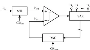
SAR ADC Advantages and Disadvantages
SAR ADCs (Successive Approximation Register ADCs) offer several advantages and disadvantages, which you should consider when choosing an ADC for your specific application. Let's explore them in detail:Advantages of SAR ADCs

Disadvantages of SAR ADCs
Limited Resolution and Linearity: While SAR ADCs can offer high resolution, they may have limitations in terms of absolute accuracy and linearity. The accuracy and linearity of SAR ADCs can be affected by factors such as noise, non-linearity in the comparator, and variations in the DAC. Careful design considerations and calibration techniques are necessary to mitigate these limitations. Conversion Speed: While SAR ADCs can achieve high sample rates, they may have slower conversion speeds compared to other ADC types such as Flash ADCs. The successive approximation process used in SAR ADCs requires multiple conversion cycles, which can result in longer conversion times. This limitation may impact applications that require extremely fast conversion rates. Susceptibility to Noise: SAR ADCs can be sensitive to noise, especially during the comparison and conversion process. Noise can introduce errors and affect the accuracy of the conversion. Proper shielding, filtering, and grounding techniques should be employed to minimize the impact of noise in SAR ADC applications. Complexity with Higher Resolutions: As the resolution of a SAR ADC increases, the complexity of the circuitry and the number of clock cycles required for conversion also increase. Higher-resolution SAR ADCs may require higher precision components and more robust design techniques, which can add complexity and cost to the overall system. Sampling Capacitance Requirements: SAR ADCs require a sampling capacitor to hold the analog input during the conversion process. The choice of the sampling capacitor affects the speed, accuracy, and power consumption of the ADC. Careful consideration and optimization of the sampling capacitor are necessary to achieve the desired performance.Conclusion
To sum up, our blog has provided insight into the captivating world of SAR ADCs.SAR ADCs are crucial in a variety of electronic systems due to their high resolution, accuracy, and efficiency. They play a significant role in converting analog signals into digital representations with precision, from microcontrollers to communication devices. We have covered their iterative approximation process, binary search algorithm, and benefits. With this understanding, you can utilize SAR ADCs' potential and capabilities in your projects and designs. Embrace their power and unleash new possibilities in the digital world.Related Articles
- ·Stratix 10 VS Stratix V: Which FPGA is Right for Your Next Project?
- ·Intel Xeon Platinum 8454H vs AMD EPYC: Which Reigns Supreme?
- ·A Deep Dive into the AMD EPYC 4564P Processor
- ·MSP430F5438A vs MSP430F5529: A Detailed Analysis of Their Capabilities
- ·Comparing MSP430F6659 and MSP430F5419A: Which One is Right for Your Project?
- ·Exploring the Features of MSP430F5529 and MSP430F5638 Microcontrollers
- ·Demystifying 20 Microcontroller Projects for Beginners
- ·Unveiling the Ultimate Guide to Microcontroller Programming
- ·4680 Battery: Unveiling the Power Potential of the Next-Gen Cell
- ·Exploring the Case Studies on Arduino Applications
Populer Posts