


Exploring 3D IC Technology: Unleashing the Power of Vertically Stacked Innovation

Global electronic component supplier AMPHEO PTY LTD: Rich inventory for one-stop shopping. Inquire easily, and receive fast, customized solutions and quotes.
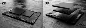
What is 3D IC Technology?
The implementation of 3D IC technology involves the vertical stacking and integration of multiple layers of electronic circuits. This process results in the creation of compact and high-performance devices that offer significant advantages over traditional electronic systems. In a standard 2D IC, the numerous components, such as transistors, resistors, and interconnects, are built on a single planar substrate, typically a silicon wafer. However, as demand for more complex and powerful electronic devices grows, the constraints of 2D ICs, such as restricted connection density, increased signal latency, and power consumption, become increasingly evident. So comes the 3D IC technology. By stacking numerous IC layers vertically and linking them with through-silicon vias (TSVs), 3D IC technology overcomes these constraints. Signals may move between the stacked layers thanks to TSVs, which are vertical electrical connections that flow through the silicon substrate. Higher connection densities, shorter interconnect lengths, lower signal delays, and better overall performance are made possible via vertical integration. The 3D IC is one of numerous 3D integration systems that take advantage of the z-direction to improve electrical performance in microelectronics and nanoelectronics.
What Are the Different Types of 3D IC?
There are different types of 3D IC technology, including: Stacked ICs: In this approach, fully processed ICs are stacked and interconnected using TSVs. Each IC layer is thinned to reduce the overall thickness of the stack, and TSVs provide electrical connections between the layers. Monolithic 3D ICs: True monolithic 3D ICs are constructed in layers on a single semiconductor wafer before being divided into 3D ICs. Because there is only one substrate, no aligning, thinning, gluing, or through-silicon vias are required. In general, monolithic 3D ICs are still a developing technology and are thought to be many years away from commercialization. This technique involves fabricating multiple layers of transistors and interconnects directly on a single silicon substrate. The layers are interconnected using TSVs, and each layer can have its own functionality, such as logic, memory, or sensors. Hybrid 3D ICs: Hybrid 3D ICs combine different types of ICs, such as stacking a logic IC layer on top of a memory IC layer. This allows for the integration of different functionalities and optimized performance.
3D IC Devices Technologies and Manufacturing
3D IC devices involve several technologies and manufacturing processes to achieve the vertical integration of multiple layers of ICs. Some key aspects are presented as follows: Through-Silicon Vias (TSVs): TSVs are vertical electrical connections that pass through the silicon substrate, enabling the interconnection between different layers of ICs in a 3D stack. TSVs are typically created by etching holes through the silicon substrate, depositing conductive material (such as copper) inside the vias, and filling them to establish electrical connections. TSVs play a crucial role in enabling vertical integration and signal transfer between the layers. Wafer Thinning: In 3D IC manufacturing, each IC layer is typically thinned to reduce the overall thickness of the stack. Thinning is achieved by removing excess silicon from the backside of the wafer, resulting in a thinner substrate. Thinning is necessary to minimize the overall thickness of the 3D stack and to maintain mechanical integrity. Die Stacking and Bonding: Once the individual IC layers are prepared, they are stacked on top of each other to form the 3D IC device. The stacking process involves aligning the layers and bonding them together. Various bonding techniques can be used, such as adhesive bonding, die-to-die bonding, or die-to-interposer bonding. These bonding processes ensure electrical connections between the stacked layers. Inter-Layer Interconnects: In addition to TSVs, inter-layer interconnects are essential for routing signals between different layers of the 3D IC stack. These interconnects can be created using techniques like redistribution layers (RDLs), which involve depositing and patterning metal layers on each IC layer to establish connections. RDLs provide a means to route signals horizontally within a layer and provide connectivity to TSVs. Thermal Management: 3D IC devices can generate higher heat densities due to the increased integration and packaging density. Effective thermal management is crucial to ensure proper device operation and reliability. Techniques such as microchannels, thermal interface materials, and heat sinks are employed to dissipate heat and maintain acceptable operating temperatures. Testing and Assembly: After the 3D IC stack is formed, it undergoes testing to ensure functionality and quality. Testing may involve electrical, functional, and reliability tests. Once the devices pass the testing stage, they are assembled into packages, which may involve encapsulation, wire bonding, or flip-chip bonding to form a final packaged 3D IC device ready for integration into electronic systems.
What’s 3D Packaging?
The technology and concept of physically stacking and fusing many comfortable chips within a single package is referred to as 3D packaging. It entails the regular calibration of satisfaction, allowing for improved functionality, command, and downsizing of electrical equipment. Volume is well-built or associated with the institute's conduct in 3D packaging, providing benefits above typical planar (2D) packaging. Valid packaging offers higher-ranking combination essence, trashy connecting lengths, improved electrical performance, and improved thermal management by exploiting the upright crevice. The shadow of 3D packaging can be found in 3D technology. Through-Silicon Vias (TSVs): TSVs are vertical electrical connections that penetrate through the silicon substrate, enabling communication between different layers or components. TSVs play a crucial role in 3D packaging by providing electrical interconnects through the vertically stacked layers. Wafer-Level 3D Packaging: This technique involves stacking and bonding multiple thinned individual chips or dies together at the wafer level. It allows for efficient batch processing and higher manufacturing yields. Package-on-Package (PoP): PoP involves stacking and interconnecting multiple packages vertically. It typically consists of a memory package stacked on top of a logic package, enabling the integration of different functionalities within a single device. Chip-on-Chip (CoC): CoC refers to the stacking and bonding of multiple chips directly on top of each other within a single package. It allows for the integration of diverse functions or technologies, such as combining a microcontroller with sensors or RF chips. Interposer-based Packaging: Interposers are passive substrates with embedded electrical connections that enable the interconnection of multiple chips or components. Interposer-based packaging provides a platform for integrating chips with different sizes, technologies, or functionalities. Fan-out Wafer-Level Packaging (FOWLP): FOWLP involves redistributing the connections from the chip to a larger area on the package substrate, allowing for increased integration density and improved electrical performance.
Challenges for 3D IC Technology
Since the technology is new and developing, it carries some challenges including: The first and paramount is of cause the cost. While lower costs are advantageous when compared to scaling, they have also been cited as a barrier to the commercialization of 3D ICs in mainstream consumer applications. However, efforts are being made to fix this. Although 3D technology is new and somewhat sophisticated, the cost of production is surprisingly simple when broken down into the activities that comprise the complete process. Cost drivers can be found by studying the mix of activities at the base. Once the cost drivers are identified, determining where the majority of the cost originates from and, more significantly, where the cost has the potential to be cut becomes a less difficult task. And the second is the testing. Testing 3D ICs poses unique challenges due to the vertical integration and complex interconnections. Developing effective test methodologies to ensure the functionality and reliability of each layer and the overall stack is essential. Testing at different stages, such as wafer-level and post-packaging, becomes more complex and time-consuming. And the third dilemma is manufacturing complexity. 3D IC manufacturing procedures are more sophisticated than typical 2D IC production processes. Through-silicon via (TSV) manufacturing, wafer thinning, and bonding all need specific equipment and expertise. Scaling up manufacturing and assuring high yields are issues that must be overcome in order for 3D IC technology to be cost-effective. Moreover, heat or thermal management is another challenge. Because of improved integration and packaging density, 3D ICs can create larger heat densities. Thermal management becomes crucial to avoiding overheating and ensuring dependable operation. Heat dissipation over vertically stacked layers and thermal hotspot mitigation are key issues in 3D IC technology.
What Are the Benefits of 3D IC Technology?
Conclusion
In summary, 3D IC technology offers a host of benefits to the field of electronics. The increased integration density, improved performance, enhanced power, and thermal management, heterogeneous integration capabilities, and design flexibility make 3D ICs well-suited for a wide range of applications. As the technology continues to advance and overcome challenges, we can expect to see even more innovative and efficient electronic devices leveraging the benefits of 3D IC technology.