


FPGA basics: Applications, Structures, and Components

Global electronic component supplier AMPHEO PTY LTD: Rich inventory for one-stop shopping. Inquire easily, and receive fast, customized solutions and quotes.
What is FPGA
The definition of "field-programmable" states that the client can program the digital logic of an integrated circuit rather than having it fixed during production. Hardware design engineers can program customized digital logic using digital ICs (integrated circuits) called field-programmable gate arrays (FPGAs). FPGAs have configurable (or programmable) logic blocks and configurable interconnects to provide this programmability. Due to their programmable logic and interconnects (routing), FPGAs are flexible and adaptable compared to ASICs of equivalent grade with conventional cells, but they are also slow and power-hungry.
Understanding FPGA Workflow and Leading ManufacturersFPGA Workflow: A Step-by-Step Guide
Field-Programmable Gate Arrays (FPGAs) are powerful devices that can be programmed to perform a wide range of logic functions. Here's a simplified workflow for working with FPGAs:
- Define the Logic Function: Using a computer, you describe the desired logic function. This can be done by drawing a schematic or creating a text file that details the function.
- Compile the Logic Function: Utilize software provided by the FPGA vendor to compile the logic function on your computer. This process generates a binary file ready for download into the FPGA.
- Download to FPGA: Connect your computer to the FPGA via a cable and download the binary file. The FPGA will then operate according to the specified logic function.
Key Points to Remember
- Unlimited Reprogramming: FPGAs can be reprogrammed as many times as needed with different functionalities. If there's a mistake in the design, simply fix the logic function, recompile, and redownload it—no need to change the PCB, solder, or components.
- High Speed: Designs run much faster within the FPGA since all operations occur on its silicon die.
- Volatility: FPGAs lose their functionality when power is lost, similar to RAM in computers. Functionality is restored by redownloading the binary file once power is back up.
Leading FPGA Manufacturers
Several companies manufacture FPGAs, with the market dominated by a few key players:
- Xilinx: The inventor of FPGAs and the largest name in the FPGA industry.
- Altera: Another heavyweight in the FPGA market, known for its robust offerings.
- Lattice: A smaller player in the FPGA market but known for its specialized products.
- Actel: Also a smaller player, offering unique FPGA solutions.
Video related to FPGA board
Different Types of PLDs
PLD is an integrated circuit (IC) that has a substantial number of logic gates and flip-flops that may be programmed to perform a wide range of functions. The logic of an array of AND and OR gates, which make up the most basic Programmable Logic Device, as well as how these gates are connected, can be programmed. PLDs can essentially be divided into three categories. As follows:
- Simple Programmable Logic Devices (SPLD)
- Complex Programmable Logic Devices (CPLD)
- Field Programmable Gate Arrays (FPGA)
Additional categories for simple programmable logic devices include PLA, PAL, and GAL. So let me see more detailed information and get more familiar with them.
Introduction to PLA
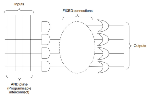
Both an AND gate plane and an OR gate plane have programmable interconnects, and together they make up a PLA. Here is a straightforward four-input, four-output PLA using AND and OR gates. By joining the horizontal and vertical connection lines, any input can be connected to any AND gate. With programmable interconnects, the outputs from several AND gates can subsequently be applied to any OR gate.

Introduction to PAL
The main difference between a PAL and a PLA is that the OR gate plane in a PAL is set during manufacture, but the AND gate plane in a PLA is programmable. PALs don't have the time delays that come with programmable OR Gates, despite being less versatile than PLAs.
Introduction to GAL
A GAL and PAL share a similar architecture, however, the distinction is in the programmable structure. While GAL utilizes EEPROM, which can be reprogrammed, PALs use PROM, which can be programmed just once.
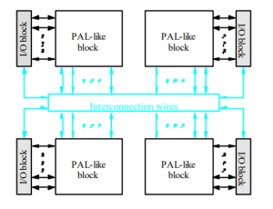
Introduction to CPLD
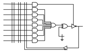
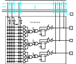
We obtain CPLD devices as a step up from SPLD devices. In order to produce much bigger and more intricate designs, it is created on top of SPLD devices. A CPLD is made up of a variety of logic blocks (also known as functional blocks), each of which internally consists of a Macrocell, a Pal, or a PAL. In order to deliver the true signal or its complement, macrocells include any additional circuitry and signal polarity control.
Introduction to FPGA
Compared to SPLDs, CPLDs are far more complex. FPGAs, however, are more intricate than CPLDs. Because it has programmable Logic Cells, programmable Interconnects, and programmable IO Blocks, an FPGA has an entirely different architecture.
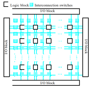
Overview of FPGA
FPGAs, or field-programmable gate arrays, are two-dimensional arrays with a matrix of reconfigurable logic circuits and programmable interconnects. Programmable interconnects (or switches), which can be created to fulfill any digital function, are used to connect the different logic cells. You can create any custom design by specifying the logic or function of each logic block and setting the connections for each programmable switch in the FPGA. The device is referred to as "field-programmable" since bespoke circuit development is carried out outside of the factory. The internal structure of the FPGA is depicted in a very general way in the pictures below. As you can see, the core of the FPGA consists of programmable interconnects and tunable logic cells. All around them are a number of programmable IO blocks used to communicate with the outside world.
FPGA Components
Now let's examine an FPGA's construction in more detail. An FPGA typically consists of three fundamental parts. As follows: Programmable Logic Cells (or Logic Blocks), Programmable Routing, and IO Blocks.
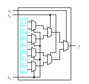
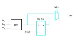
Logic Block
While identical structures in Altera-based FPGAs are known as Logic Array Blocks or LAB, the logic block in Xilinx-based FPGAs is referred to as Configurable Logic Blocks or CLB. Let's refer to CLB in this conversation. The fundamental part of an FPGA that has both logic and storage capabilities is called a CLB. Transistors, NAND gates, multiplexors, look-up tables (LUTs), PAL-like structures, or even processors can all be used as the basic logic block. Look-up Table (LUT) based logic blocks are used by both Xilinx and Altera to implement the logic and storage functionalities. A Basic Logic Element is a mix of a Look-up table (which is made up of SRAM and Multiplexors) and a Flip-flop, and a Basic Logic Element can be one Basic Logic Element or a set of interconnected Basic Logic Elements. SRAM Cells are used to implement the 2n configuration bits that make up a LUT with 'n' inputs. The LUT can be designed to implement any logical function using these 2n SRAM Bits.
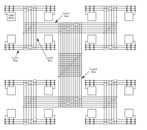
Programmable Routing
If the Logic Blocks are in charge of providing the computational functionality, the programmable routing network is in charge of connecting the Logic Blocks. To fully design a bespoke circuit, the routing network offers connections between each logic block as well as between the logic block and the IO Block. The routing network essentially consists of joining lines with programmable switches that may be set up using any computer language. Routing architectures generally fall into one of two categories. They are hierarchical routing and island-style routing. The logic blocks are organized in a two-dimensional array and connected using a programmable routing network in an island-style routing architecture. In commercial FPGAs, this kind of routing is commonly utilized. By grouping the logic blocks into several groups or clusters, hierarchical routing architecture makes use of the fact that many logic blocks are restricted to a local set of connections. The hierarchical routing connects the logic blocks at a low level of hierarchy if they are housed in the same cluster. When logic blocks are distributed across various clusters, wiring is carried out at a higher level of the hierarchical structure.
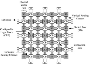
IO Blocks
The interface between FPGA and external circuits is the programmable input and output unit known as the IOB (Input Output Block). used to fulfill the criteria for driving and matching input/output signals under various electrical characteristics. The IOB of an FPGA is split up into many banks to aid in management and allow for adaption to various electrical standards. Each bank's interface voltage VCCO determines its interface standard. There can only be one VCCO per bank, however, there can be multiple VCCOs for the same bank. Only ports that adhere to the same electrical standard can be linked. The fundamental requirement of the interface standard is the identical VCCO voltage.
Technology for Programming FPGAs
We've discussed a lot about the FPGAs' reprogrammable architecture, but now let's look at some of the most popular programming methods that gave rise to this kind of reconfigurable architecture. Three well-known programming techniques that are utilized in FPGAs are Anti-Fuse, EEPROM/Flash, and SRAM.
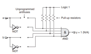
Anti-Fuse
An ancient method of creating once-programmable electronics is anti-fuse programming. They are implemented by means of an anti-fuse link, which has an extremely high resistance in its unprogrammed condition and functions as an open circuit. High voltage and current are applied to the input during programming. The anti-fuse then comes to life by changing into a conducting polysilicon from its initial state of amorphous silicon, which is essentially an insulator with very high resistance connecting two metal tracks. The anti-fuse technology takes up the least area when compared to the other two, however, it is only available as a once-only programmed option.
EEPROM/Flash
Based on EEPROM or Flash programming technologies, SRAM-based programming technology has a strong competitor. Flash-based programming's primary benefit is that it is non-volatile. Despite the fact that flash offers re-programmability, it can only be done a relatively tiny number of times compared to SRAM technology.
SRAM
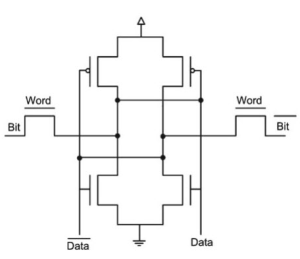
We are aware that semiconductor RAM comes in two varieties: SRAM and DRAM. While DRAM stands for dynamic RAM, SRAM stands for static RAM. The term static refers to the fact that a basic SRAM Memory Cell's value will not change unintentionally or when the power is turned off. SRAM is constructed utilizing transistors. The following graphic displays an example of a typical six-transistor SRAM cell for storing one bit. Unlike the DRAM, which combines a transistor and a capacitor, this is not the case. The term "dynamic" describes the property that the value stored in the fundamental DRAM Memory Cell remains valid as long as the capacitor is charged. The memory cell must be routinely refilled to keep its charge because capacitors gradually lose charge. Refreshing is another name for this. For programming, many FPGA vendors use Static Memory Cells in SRAM-based FPGAs. SRAM-based FPGAs have gained popularity because to their re-programmability and use of CMOS technology, which is known for its low dynamic power consumption, high speed, and tighter integration. They are used to program both the logic cells and the interconnects.
FPGA-Based Project
- IEEE 802.16e FPGA Implementation of the FFT Algorithm (Mobile WiMAX)
- Designing GPS (Global Positioning System)-GSM Using FPGA (Global Systems for Mobiles)
- LabVIEW implementation of Mobile Navigator Space Vector PWM (Pulse Width Modulation) for Three-Level Converters
- Field Oriented Control Development and Evaluation Using LabVIEW Design and
- Implementation of Programmable Multi-Processor Platform for High Performance
- MIMO Sphere System Implementation and Architecture
- FPGA-based High-Frequency Carrier Generation for Pulse Compression Using Cordic Algorithm
- Design and Synthesis of Programmable Logic Blocks Using Macro Gates and Mixed LUT
- Design and implementation of MP4 decoders using FPGA
FPGA Applications
- Wireless Communications
- Wired Communications
- Video & Image Processing
- Security
- Medical
- High-Performance Computing and Data Storage
- Consumer Electronics
- Broadcast & Pro AV
- ASIC Prototyping
Ⅸ FPGA board FAQ
What is the FPGA?
FPGAs are integrated circuits that are frequently available off-the-shelf. Because they enable customers to modify the hardware to satisfy certain use case needs after the production process, they are referred to as "field-programmable."
What are the differences between FPGA and MCU?
An FPGA and a microcontroller differ primarily in their degree of customization and complexity. Price and usability variations are also present. In essence, an FPGA enables more sophisticated operations, higher levels of customization, and hardware changes that may be made after the fact.
What are the differences between FPGA and CPLD?
An integrated circuit called a CPLD aids in the operation of digital systems. An FPGA, on the other hand, is an integrated circuit that is primarily made to be altered by a customer or a developer after production. Up to 100,000 tiny logic blocks can be found in FPGAs.
What can be FPGA used for?
an be reprogrammed to meet specific application or feature needs. Among the industries that use FPGAs include aerospace and defense, wireless communications, digital television, consumer electronics, industrial motor control, and scientific equipment.
Related Articles
- ·How to boot Linux on a Xilinx FPGA?
- ·Is FPGA chip suitable for algorithm development?
- ·The best MCUs/MPUs for industrial humanoid robots
- ·What are the differences between FPGA and DSP processors for signal processing?
- ·How to become an FPGA engineer? Which FPGA board and program are suitable for beginners?
- ·How to Generate Low Clock Frequencies in FPGA?
- ·How to Use DDR Memory with FPGA for DSP Application?
- ·Application of Embedded Systems in Aerospace and Defense Fields
- ·Comparison of FPGA, ARM, STM32, and DSP Platforms
- ·Comparison of FPGA, CPLD, PLC, Microprocessor, Microcontroller & DSP