

In this blog, we'll delve into the world of Manifold Absolute Pressure (MAP) sensors, uncovering their secrets and unraveling their vital role in y...
View detailsSurface Mount Technology (SMT) Basic and Its Process
blog 765
In this blog, we aim to provide an in-depth overview of Surface Mount Technology (SMT), a method of electronic component assembly that has transformed the electronics industry. We will delve into the fundamental aspects of SMT, including its advantages over traditional through-hole technology, and the process involved in SMT. Whether you are an experienced engineer or new to electronics, this article will furnish you with valuable insights into this critical technology.
What is Surface Mount Technology (SMT)?
The electronics industry has been transformed by Surface Mount Technology (SMT), which is a technique for assembling electronic components. It involves mounting electronic components directly onto the surface of a printed circuit board (PCB), rather than inserting them into holes drilled in the PCB. This allows for smaller and more densely packed electronic devices, as well as faster and more automated assembly processes. SMT has become the industry standard over the past several decades and is used in a wide range of applications, from consumer electronics to medical devices to aerospace and defense systems.
The development of SMT has been driven by the need for smaller, more powerful, and more reliable electronic devices. In the early days of electronics, through-hole technology was the norm, with components inserted into holes drilled in the PCB and then soldered in place. This worked well for larger devices, but as electronics became more miniaturized, it became clear that a new approach was needed.
SMT was developed in the 1960s and 1970s as a way to address these challenges. By mounting components directly onto the surface of the PCB, it became possible to create much smaller and more densely packed devices. This allowed for the development of new technologies, such as smartphones, laptops, and other portable electronic devices that have become ubiquitous in modern life.
Today, SMT is used in virtually all electronic devices, from simple toys to complex medical equipment. It has enabled the development of new technologies, such as flexible and stretchable electronics, that were once thought impossible. As the electronics industry continues to evolve, it is clear that SMT will remain a critical technology for years to come.
What Does An SMT Do?
SMT, or Surface Mount Technology, is a method of electronic component assembly that involves mounting electronic components directly onto the surface of a printed circuit board (PCB). SMT machines are used to automate the assembly process of electronic devices, placing electronic components onto the PCB quickly and accurately.
SMT machines use a variety of techniques to place components onto the PCB, including pick-and-place machines, stencil printers, and reflow ovens. Pick-and-place machines use robotic arms to pick up components from a feeder and place them onto the PCB in the correct position. Stencil printers are used to apply solder paste to the PCB, which acts as an adhesive for the components. Reflow ovens are used to heat the PCB and melt the solder paste, securing the components in place.
SMT machines can place hundreds or even thousands of components per minute, depending on the complexity of the device being assembled. This makes it possible to produce electronic devices in large quantities quickly and efficiently. SMT has revolutionized the electronics industry, making it possible to produce smaller, more powerful, and more reliable devices than ever before.
Surface Mount Technology (SMT) Process
Generally speaking, the SMT process contains the followings procedures:
PCB Preparation
PCB Design: The PCB layout is designed using computer-aided design (CAD) software. This includes determining component placement areas, routing traces, and creating solder pads or lands for component connections.
Gerber Files: The PCB design is exported to Gerber files or other manufacturing data formats that PCB fabrication houses can use.
Stencil Creation
Stencil Design: A stencil is created with openings corresponding to the solder pads on the PCB. The stencil can be made of stainless steel or polymer materials.
Stencil Alignment: The stencil is aligned and secured over the PCB using a fixture or clamps.
Solder Paste Application
Solder Paste Selection: A solder paste, consisting of a mixture of flux and tiny solder particles, is selected based on the application and component requirements.
Solder Paste Printing: The solder paste is applied to the PCB through the openings in the stencil using a squeegee or a solder paste dispenser.
Squeegee Method: A squeegee blade is used to spread the solder paste over the stencil, pushing it through the openings onto the solder pads.
Dispensing Method: Solder paste is dispensed through a controlled mechanism, depositing precise amounts onto the solder pads.
Component Placement
Pick-and-Place Machine: Automated pick-and-place machines are used to accurately position the electronic components onto the solder paste-covered pads on the PCB.
Feeder Setup: Component reels, tubes, or trays are loaded onto the pick-and-place machine's feeders, which supply the components during the placement process.
Vision System Alignment: Vision systems on the pick-and-place machine locate fiducial marks on the PCB to ensure accurate component placement.
Component Placement: Vacuum nozzles on the machine pick up the components and place them in the designated locations on the PCB.
Reflow Soldering
Conveyor Belt or Reflow Oven: The PCB with components is transferred to a conveyor belt that passes through a reflow oven.
Heating Zones: The reflow oven typically has multiple heating zones, each with controlled temperature profiles.
Preheat Zone: The PCB enters the preheat zone, gradually raising the temperature to remove moisture and activate the flux in the solder paste.
Reflow Zone: The PCB moves into the reflow zone, where the temperature is raised to melt the solder paste and create solder joints.
Cooling Zone: The PCB then moves into the cooling zone, where it gradually cools, solidifying the solder joints.
Inspection and Quality Control
Automated Optical Inspection (AOI): After reflow soldering, an AOI system scans the PCB to detect defects such as missing components, misalignment, solder bridging, or insufficient solder.
X-ray Inspection: X-ray inspection may be used to examine hidden solder joints or verify the integrity of ball grid array (BGA) packages.
Manual Inspection: Skilled technicians may perform manual inspections to ensure the quality of solder joints and components.
Testing and Functional Verification
Electrical Testing: The assembled PCB may undergo functional testing or electrical tests to verify its performance and integrity.
Boundary Scan Testing: Boundary scan testing is performed to test the interconnections between components on the PCB using standardized protocols.
Additional Manufacturing Processes
Conformal Coating: A protective conformal coating may be applied to the PCB to safeguard it against environmental factors such as moisture, dust, or chemicals.
Cleaning: The PCB may undergo a cleaning process to remove any flux residue or contaminants left after soldering.
Encapsulation: Some electronic assemblies may require encapsulation or potting with a protective compound for additional mechanical strength or environmental protection.
Throughout the SMT process, quality control measures are essential to ensure reliable and high-quality PCB assemblies. These measures include proper solder paste inspection, component traceability, and adherence to industry standards and specifications.
SMD vs SMT vs THT
SMD, SMT, and THT are three different methods of mounting electronic components onto printed circuit boards (PCBs). Even though, there are some differences between them.
| Feature | SMD (Surface Mount Device) | SMT (Surface Mount Technology) | THT (Through-Hole Technology) |
| Component Type | Small, flat, rectangular shape | Various shapes and sizes | Various shapes and sizes |
| Mounting Method | Surface mounted on PCB | Surface mounted on PCB | Inserted through drilled holes |
| Component Density | High | High | Relatively lower |
| PCB Complexity | Supports complex PCB designs | Supports complex PCB designs | Supports complex PCB designs |
| Manufacturing Speed | Faster assembly process | Faster assembly process | Slower assembly process |
| Automation | Highly automated process | Highly automated process | Manual or automated |
| Repair and Rework | More challenging | More challenging | Easier |
| Mechanical Strength | Moderate to high | Moderate to high | High |
| Space Requirement | Occupies less space on PCB | Occupies less space on PCB | Requires more space on PCB |
| Application | Widely used in modern devices | Widely used in modern devices | Used in specific applications |
Advantages of SMT
SMT revolutionized the electronics industry by offering numerous advantages over traditional through-hole technology. SMT has become the preferred method for mounting electronic components onto printed circuit boards (PCBs) due to its remarkable benefits.
One of the primary advantages of SMT is its ability to drastically reduce the size and weight of electronic devices. SMT components are smaller and lighter compared to through-hole components, allowing for compact and lightweight designs. This miniaturization is especially advantageous in portable and space-constrained applications.
SMT also enables higher component density on PCBs. With smaller components and the ability to mount them on both sides of the PCB, SMT offers increased design flexibility and the ability to pack more functionality into a smaller area. This advantage has paved the way for the development of smaller, more powerful electronic devices.
In addition to size reduction, SMT offers improved electrical performance. The shorter lead lengths and reduced parasitic capacitance and inductance of SMT components result in better signal integrity, reduced noise, and enhanced high-frequency performance. This makes SMT ideal for applications requiring high-speed and high-frequency circuits.
Another significant advantage of SMT is its manufacturing efficiency. The use of pick-and-place machines for component placement and reflow soldering techniques enables faster and more automated assembly processes. This leads to higher production throughput, cost-effectiveness, and streamlined manufacturing operations.
SMT also contributes to increased reliability in electronic assemblies. The smaller solder joints and larger surface area connections of SMT components offer stronger and more reliable electrical and mechanical connections. SMT components are more resistant to mechanical stress, vibration, and thermal cycling issues, resulting in enhanced durability and reliability.
Furthermore, SMT can bring cost savings. The smaller size of SMT components reduces raw material costs, while automated assembly processes and improved manufacturing efficiency contribute to lower production and assembly costs.
With its design flexibility, compatibility with advanced technologies and a host of other advantages, SMT has become the backbone of modern electronics manufacturing. It has enabled the development of smaller, lighter, more efficient, and reliable electronic devices with improved performance and functionality, driving innovation across various industries.
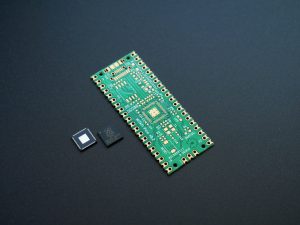
Figure 1 SMT
Conclusion
Surface Mount Technology (SMT) has emerged as the prevailing industry standard for electronic component assembly, boasting a multitude of advantages over traditional through-hole technology. By directly affixing components onto the surface of a printed circuit board (PCB), SMT facilitates the creation of smaller, more densely packed electronic devices, while expediting and automating assembly processes.
The SMT assembly process encompasses stencil printing, pick-and-place procedures, reflow soldering, and meticulous inspection. Remarkably, SMT machines are capable of placing hundreds, or even thousands, of components per minute, thereby enabling the rapid and efficient production of electronic devices in substantial quantities.
Undoubtedly, SMT has revolutionized the electronics sector, empowering the realization of technological breakthroughs and applications that were once deemed unattainable. From smartphones and medical devices to aerospace and defense systems, SMT has paved the way for the fabrication of electronic devices that are not only smaller but also more potent and reliable than ever before. As the electronics industry continues its evolution, the enduring significance of SMT as a critical technology becomes increasingly apparent, poised to shape the landscape of electronics for years to come.
Becky
Becky is a technical writer who are interested in writing some professional and original articles. She spent some time working in some electronic sector, but her main area of interest is the use of AI in edge computing. The rest of the time, she write or program about technology-related articles pertaining to the Internet of Things, GPU computing, LoraWAN, PCB, Machine Learning, Precision Agriculture, Open Electronics, and similar areas.
WEW ALL POSTS BYBeckyRelated Articles
-
 Unveiling MAP Sensors: What They Are and How They Work 284
 -
 Microcontroller vs. Microprocessor vs.Microcomputer: Which is Better? 588
Microcontrollers, microprocessors, and microcomputers are all essential components in many electronic devices. In this blog, we will discuss the ke...
View details -
 MOSFET vs IGBT: Which One is Better? 331
High-power electrical signals are controlled and switched by Mosfets (Metal-Oxide-Semiconductor Field-Effect Transistors) and IGBTs (Insulated Gate...
View details -
 What is An Optical Isolator? 210
In this blog, we will briefly talk about the basics of optical isolators.
View details -
 Raspberry Pi vs Asus Tinker Board: Advantages and Disadvantages 150
In the vibrant world of single-board computers (SBCs), two titans reign supreme: Raspberry Pi and Asus Tinker Board. In this blog, we will dive dee...
View details -
 All you Need to Know about Capacitive Reactance 579
Capacitive reactance is thoroughly explored in this article, which covers its definition, formula, and determining factors.The influence of frequen...
View details