


Clock Management in FPGAs/CPLDs

Global electronic component supplier AMPHEO PTY LTD: Rich inventory for one-stop shopping. Inquire easily, and receive fast, customized solutions and quotes.
FPGAs/CPLDs Introduction
Of the four signal groups in digital design - internal signals, I/O signals, reset, and clock - the latter has the highest requirements for signal quality and timing. Deficiencies in the clock network can lead to unwanted, often catastrophic behavior of the circuit. To avoid this, special design rules have been formulated and components developed for clock distribution in digital circuits. The methods for signal routing in ASICs and FPGAs differ in detail and also differ from the requirements and methods for external signal routing on PCBs.
Basic Requirements for Clock Networks
The clock must be distributed to all clocked elements (flip-flops, RAMs, I/O cells) in the IC (ASIC / FPGA) with minimal distortion and must be able to drive a very large number of gate inputs (up to several hundred thousand!). The propagation delay from the chip input to each endpoint of the network should ideally be exactly the same. This ensures that all flip-flops switch at approximately the same time, guaranteeing high synchronicity. The remaining unavoidable differences are accounted for by the tools, which provide sufficient time margins. The difference in propagation delay between different endpoints of the clock network is called skew and ideally lies below 100ps in modern digital circuits.
To achieve this, a number of measures are taken:
Special input buffers are provided at the inputs of PLDs, FPGAs, and ASICs, which can sometimes be fed by symmetric signal sources.
Different clock networks and clock regions are provided in PLDs and FPGAs. In ASICs, these are created as needed.
Global and sometimes regional clock drivers are used (in Xilinx FPGAs: BUFG).
Clock networks are often designed as tree structures (i.e., equal length from the tree root to each branch tip). This circuit technique is therefore also called a "Clock Tree".
Clock Domains / Clock Generation
In almost every digital circuit, different areas should not perform an action on every clock cycle or work at a significantly lower clock rate than the rest of the circuit. For this purpose, a slow clock must be derived from the relatively fast system clock. What looks simple at first glance is often done incorrectly in detail.
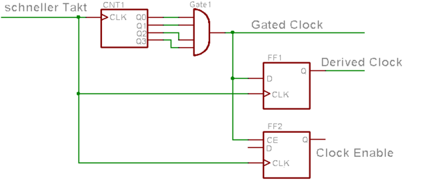
Gated Clocks
This term refers to switched, i.e., interrupted ("gated"), clock lines. This can happen through the use of:
- Multiplexers (selection between clock source 1 and 2) or
- Combinatorial logic (circuit parts are disconnected from the clock under certain conditions)
Clock Enable
Every flip-flop in FPGAs/CPLDs has a synchronous control input called CE (Clock Enable). This allows you to specify whether the flip-flop should store new data or keep the old data on the next clock edge. Since it is a synchronous input, it is completely uncritical if this signal contains glitches.
Examples
Here is the optimized VHDL code for using "Clock Enable" that aligns with the habits of an English-speaking audience:
library IEEE;
use IEEE.STD_LOGIC_1164.ALL;
use IEEE.NUMERIC_STD.ALL;
entity clock_enable_example is
Port ( clk : in std_logic;
reset : in std_logic);
end clock_enable_example;
architecture Behavioral of clock_enable_example is
constant CNT_DIV: integer := 16; -- Clock divide ratio
signal cnt: integer range 0 to CNT_DIV-1; -- Counter for clock division
signal ce: std_logic;
begin
-- Process with slow clock enable
process(clk)
begin
if rising_edge(clk) then
if ce = '1' then
-- Insert actions here that run with the slow clock
-- Example: Output a message
report "Clock Enable is active!";
end if;
end if;
end process;
-- Clock Enable Generator
process(clk)
begin
if rising_edge(clk) then
if reset = '1' then
ce <= '0';
cnt <= 0;
else
if cnt = CNT_DIV - 1 then
ce <= '1';
cnt <= 0;
else
ce <= '0';
cnt <= cnt + 1;
end if;
end if;
end if;
end process;
end Behavioral;
Signal and Constant Declarations:
CNT_DIV: The divide ratio for generating the clock enable signal (ce). In this example, the clock enable signal is activated every 16 clock cycles.
cnt: The counter used to generate the clock enable signal.
ce: The clock enable signal.
Process for Slow Clock Enable Actions:
This process is triggered on the rising edge of the input clock (clk).
When the clock enable signal (ce) is '1', the desired actions are executed. Here, an example message is output.
Clock Enable Generator:
This process is also triggered on the rising edge of the input clock (clk).
The counter (cnt) increments with each clock cycle until it reaches the value CNT_DIV - 1.
When the counter reaches CNT_DIV - 1, the clock enable signal (ce) is set to '1' and the counter is reset.
Otherwise, the clock enable signal (ce) remains '0' and the counter continues to increment.
A reset signal (reset) is added to initialize the counter and clock enable signal when necessary.
Clock Skew
Using the clock skew setting, a synthesis tool can be instructed to adjust the timing of the clock edge according to the requirements of the circuit delays. This creates more reserves.
Phase Shift
Within the FPGA PLLs, multiple clocks can be derived from the same input clock, which have a fixed shift. This shift is the main tool for establishing the required timing for a rising edge of an internal clock in relation to externally incoming data and compensating for propagation delays in the FPGA and I/O banks.
Related Articles
- ·What are some common Arduino projects for beginners?
- ·How do you set up a Raspberry Pi as a VPN server?
- ·How are FPGAs used in AI/ML applications?
- ·STM32 four precision control methods for stepper motors
- ·What is the lowest power STM32 MCU? how to choose?
- ·How to boot Linux on a Xilinx FPGA?
- ·Blue Pill vs Black Pill: What’s the Difference and How to Choose?
- ·The Application of Sensors in Smart Home Appliances
- ·What are the reasons for electronic component failure?
- ·Why can STM32 stand out from many 32-bit microcontrollers?