


AMD
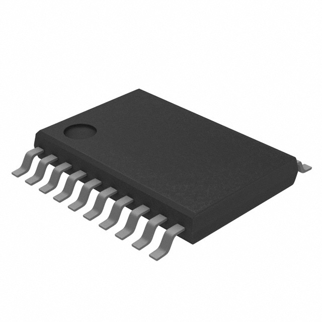
XCF02SVO20C
FPGAs (Field Programmable Gate Array)
XCF02SVO20C
2-XCF02SVO20C
FPGA Configuration PROM Memory
In Stock : Please Submit RFQ TO US
Need wholesale pricing? Send RFQ now for the best rates and immediate response.
QUICK RFQ
ADD TO RFQ LIST
XCF02SVO20C Description
Tech Specifications
Factory Lead Time
10 Weeks
Contact Plating
Lead, Tin
Mount
Surface Mount
Mounting Type
Surface Mount
Package / Case
20-TSSOP (0.173, 4.40mm Width)
Number of Pins
20
Operating Temperature
-40??C~85??C
Packaging
Tube
Published
1999
Data Retention Time-Min
20
Number of Terminations
20
Operating Supply Voltage
3.3V
ECCN Code
EAR99
Supply Voltage-Max (Vsup)
3.6V
Supply Voltage-Min (Vsup)
3V
Programmable Type
In System Programmable
Terminal Finish
Tin/Lead (Sn85Pb15)
Memory Size
2Mb
Supply Current-Max
0.01mA
JESD-609 Code
e0
Organization
2MX1
Memory Width
1
Voltage - Supply
3V~3.6V
Terminal Position
DUAL
Terminal Form
GULL WING
Peak Reflow Temperature (Cel)
225
Standby Current-Max
0.001A
Number of Functions
1
Supply Voltage
3.3V
Pbfree Code
no
Terminal Pitch
0.65mm
Part Status
Active
Time@Peak Reflow Temperature-Max (s)
30
Base Part Number
XCF*S
Pin Count
20
Parallel/Serial
SERIAL
Moisture Sensitivity Level (MSL)
3 (168 Hours)
Memory IC Type
CONFIGURATION MEMORY
Length
6.5024mm
Height Seated (Max)
1.19mm
Width
4.4mm
Radiation Hardening
No
RoHS Status
Non-RoHS Compliant
Lead Free
Contains Lead
XCF02SVO20C Documents
Download datasheets and manufacturer documentation for XCF02SVO20C
Related Parts
M1AGL1000V5-CSG281
Microsemi
A1415A-PLG84M
Microsemi
XCV600-5BGG560C
AMD
XC95216-3HQ208I
AMD
M1A3P250-2VQ100I
Microsemi
A1225A-PLG84C
Microsemi
QL8X12B-2PL68I
QuickLogic
XCV1000E-BG560C
AMD
M1AGL250V2-VQG100
Microsemi
XCV200E-8FG1156C
AMD
XC9572-10PC44ASJ
AMD
XCMECH-FF1738
AMD
XCS30-3PQ240I
AMD
A3PE3000L-FG896
Microsemi
M1A3PE3000L-PQG208
Microsemi
A42MX24-PL84
Actel
Shopping Guide
Payment Methods
Payment Methods include Prepayment TT (bank transfer), Western Union, and PayPal. Customers are responsible for shipping costs, bank charges, customs duties and taxes.
Shipping Rate
Shipments are made once a day around 5pm, excluding Sundays. Once shipped, the estimated delivery time is usually 5-7 business days, depending on the courier you choose.
Delivery Methods
Provide DHL, FedEx, UPS, EMS, SF Express and Registered Airmail International Delivery Service
Follow Us
Please find more information about us from below social media and interact with us!
Contact With Us
TOOLS
payment
Transportation
Trademark
All Rights Reserved © 2025 AMPHEO PTY LTD