


AMD
XC6VLX75T-2FF784I
FPGAs (Field Programmable Gate Array)
XC6VLX75T-2FF784I
2-XC6VLX75T-2FF784I

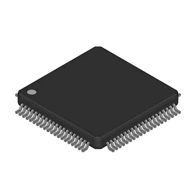
FPGA Virtex-6 LXT Family 74496 Cells 40nm Technology 1V 784-Pin FCBGA
In Stock : Please Submit RFQ TO US
Need wholesale pricing? Send RFQ now for the best rates and immediate response.
QUICK RFQ
ADD TO RFQ LIST
XC6VLX75T-2FF784I Description
Tech Specifications
Min Operating Temperature
0°C
Min Supply Voltage
950mV
Mount
Surface Mount
Max Supply Voltage
1.05V
Terminal Finish
TIN LEAD
Terminal Position
BOTTOM
Package / Case
FCBGA
Specifications
Value
Technology
CMOS
JESD-30 Code
S-PBGA-B784
Number of Inputs
360
Terminal Form
BALL
Number of Terminations
784
Supply Voltage
1V
ECCN Code
3A991.D
Number of Logic Elements/Cells
74496
Qualification Status
Not Qualified
Pbfree Code
no
RoHS Status
RoHS Compliant
RAM Size
702kB
Number of Logic Blocks (LABs)
5820
Number of I/O
360
JESD-609 Code
e0
Pin Count
784
Number of Outputs
360
Time@Peak Reflow Temperature-Max (s)
NOT SPECIFIED
Max Operating Temperature
85°C
Peak Reflow Temperature (Cel)
NOT SPECIFIED
Programmable Logic Type
FIELD PROGRAMMABLE GATE ARRAY
Subcategory
Field Programmable Gate Arrays
Contact Plating
Lead, Tin
Speed Grade
2
Terminal Pitch
1mm
Temperature Grade
OTHER
XC6VLX75T-2FF784I Documents
Download datasheets and manufacturer documentation for XC6VLX75T-2FF784I
Related Parts
XCV50-6FG256CES
AMD
COREDES-RU
Actel
XCV50E-5PQ240C
AMD
QL2007-2PF144C
QuickLogic
APA450-FGG256
Actel
M2S010TS-VFG400
Microsemi
M1AGL1000V5-FG256
Microsemi
QL2003-XPF100C
QuickLogic
XC9572-15PQ44C
AMD
XC5206-7PQ160C
AMD
XCR3064XL-7CP56I
AMD
RTAX1000SL-1LG624V
Actel
XCV1600E-5FG680C
AMD
XCV100-6FGG256I
AMD
Shopping Guide
Payment Methods
Payment Methods include Prepayment TT (bank transfer), Western Union, and PayPal. Customers are responsible for shipping costs, bank charges, customs duties and taxes.
Shipping Rate
Shipments are made once a day around 5pm, excluding Sundays. Once shipped, the estimated delivery time is usually 5-7 business days, depending on the courier you choose.
Delivery Methods
Provide DHL, FedEx, UPS, EMS, SF Express and Registered Airmail International Delivery Service
Follow Us
Please find more information about us from below social media and interact with us!
Contact With Us
TOOLS
payment
Transportation
Trademark
All Rights Reserved © 2025 AMPHEO PTY LTD