


AMD
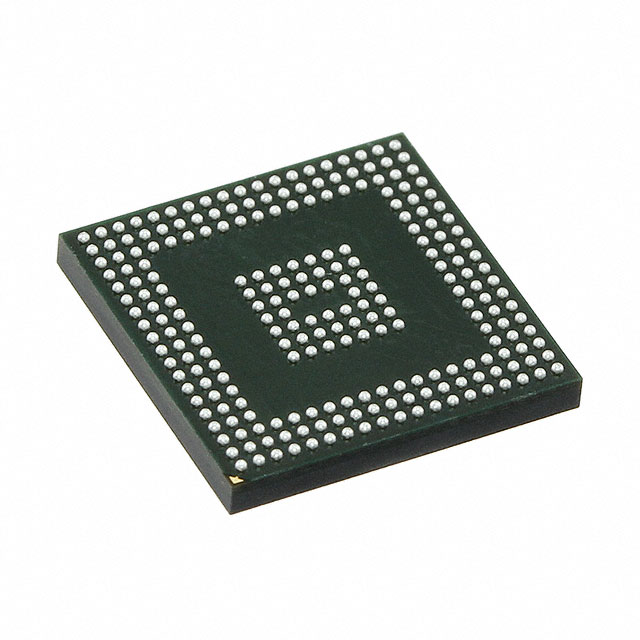
XC6VLX550T-2FFG1759I
FPGAs (Field Programmable Gate Array)
XC6VLX550T-2FFG1759I
2-XC6VLX550T-2FFG1759I

FPGA Virtex-6 LXT Family 549888 Cells 40nm Technology 1V 1759-Pin FCBGA
In Stock : Please Submit RFQ TO US
Need wholesale pricing? Send RFQ now for the best rates and immediate response.
QUICK RFQ
ADD TO RFQ LIST
XC6VLX550T-2FFG1759I Description
Tech Specifications
Operating Temperature-Min:
-40 °C
Pin Count:
1759
Length:
42.5 mm
Terminal Form:
BALL
Supply Voltage-Max:
1.05 V
Part Package Code:
BGA
Subcategory:
Field Programmable Gate Arrays
Reach Compliance Code:
not_compliant
Rohs Code:
Yes
Package Shape:
SQUARE
Package Code:
BGA
Terminal Pitch:
1 mm
Specifications
Value
Package Description:
BGA, BGA1759,42X42,40
Pbfree Code:
Yes
JESD-30 Code:
S-PBGA-B1759
Ihs Manufacturer:
XILINX INC
Part Life Cycle Code:
Active
Temperature Grade:
INDUSTRIAL
Manufacturer:
Xilinx
Manufacturer Part Number:
XC6VLX550T-2FFG1759I
Operating Temperature-Max:
100 °C
HTS Code:
8542.39.00.01
Surface Mount:
YES
JESD-609 Code:
e1
Package Style:
GRID ARRAY
Peak Reflow Temperature (Cel):
245
Terminal Finish:
Tin/Silver/Copper (Sn96.5Ag3.0Cu0.5)
Package Body Material:
PLASTIC/EPOXY
Risk Rank:
5.21
Number of Outputs:
840
Supply Voltage-Min:
0.95 V
Technology:
CMOS
Number of Inputs:
840
Supply Voltage-Nom:
1 V
ECCN Code:
3A001.A.7.A
Number of Terminals:
1759
XC6VLX550T-2FFG1759I Documents
Download datasheets and manufacturer documentation for XC6VLX550T-2FFG1759I
Related Parts
AGLE3000V5-FGG484
Actel
A1280XLTQ176
Actel
RTAX250S-1CQ352V
Actel
M2S060TS-VF400
Microsemi
APA600-PQG208M
Actel
A3P600L-1FGG144
Microsemi
XCS10-4VQ100I
AMD
XCV200-4BG256CES
AMD
XC95288-10FG256C
AMD
AX250-1FGG484M
Actel
Shopping Guide
Payment Methods
Payment Methods include Prepayment TT (bank transfer), Western Union, and PayPal. Customers are responsible for shipping costs, bank charges, customs duties and taxes.
Shipping Rate
Shipments are made once a day around 5pm, excluding Sundays. Once shipped, the estimated delivery time is usually 5-7 business days, depending on the courier you choose.
Delivery Methods
Provide DHL, FedEx, UPS, EMS, SF Express and Registered Airmail International Delivery Service
Follow Us
Please find more information about us from below social media and interact with us!
Contact With Us
TOOLS
payment
Transportation
Trademark
All Rights Reserved © 2025 AMPHEO PTY LTD