


AMD
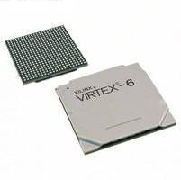
XC6VLX365T-3FF1156C
FPGAs (Field Programmable Gate Array)
XC6VLX365T-3FF1156C
2-XC6VLX365T-3FF1156C

FPGA Virtex-6 LXT Family 364032 Cells 40nm Technology 1V 1156-Pin FCBGA
In Stock : Please Submit RFQ TO US
Need wholesale pricing? Send RFQ now for the best rates and immediate response.
QUICK RFQ
ADD TO RFQ LIST
XC6VLX365T-3FF1156C Description
Tech Specifications
Clock Frequency
1412MHz
Mount
Surface Mount
Terminal Position
BOTTOM
Package / Case
1156-BBGA, FCBGA
Specifications
Value
Technology
CMOS
JESD-30 Code
S-PBGA-B1156
Voltage - Supply
0.95V~1.05V
Number of Inputs
600
Terminal Form
BALL
Supply Voltage
1V
Number of Logic Elements/Cells
364032
Qualification Status
Not Qualified
RoHS Status
Non-RoHS Compliant
Moisture Sensitivity Level (MSL)
4 (72 Hours)
Operating Temperature
0°C~85°C TJ
RAM Size
1.8MB
Total RAM Bits
15335424
Number of LABs/CLBs
28440
Number of I/O
600
Mounting Type
Surface Mount
JESD-609 Code
e0
Power Supplies
11.2/2.5V
Number of Outputs
600
Time@Peak Reflow Temperature-Max (s)
NOT SPECIFIED
Peak Reflow Temperature (Cel)
NOT SPECIFIED
Series
Virtex®-6 LXT
Programmable Logic Type
FIELD PROGRAMMABLE GATE ARRAY
Subcategory
Field Programmable Gate Arrays
Operating Supply Voltage
1V
Packaging
Tray
Part Status
Active
Published
2008
Speed Grade
3
Terminal Pitch
1mm
Reach Compliance Code
not_compliant
Base Part Number
XC6VLX365T
XC6VLX365T-3FF1156C Documents
Download datasheets and manufacturer documentation for XC6VLX365T-3FF1156C
Related Parts
M1A3P600-1FG256I
Microsemi
XC6SLX45-3FG676C
AMD
XCR5032-10PC44C
AMD
XCR3128-15PQ100C
AMD
A3265DXP-PL84
Actel
XCS10-4T144C
AMD
XCDAISY-FF1738
AMD
XCV100-6CSG144C
AMD
XCV50E-PQ240AGT
AMD
QL8050-6PT196C
QuickLogic
A42MX16-2PLG84
Microsemi
A42MX16-2VQG100I
Microsemi
Shopping Guide
Payment Methods
Payment Methods include Prepayment TT (bank transfer), Western Union, and PayPal. Customers are responsible for shipping costs, bank charges, customs duties and taxes.
Shipping Rate
Shipments are made once a day around 5pm, excluding Sundays. Once shipped, the estimated delivery time is usually 5-7 business days, depending on the courier you choose.
Delivery Methods
Provide DHL, FedEx, UPS, EMS, SF Express and Registered Airmail International Delivery Service
Follow Us
Please find more information about us from below social media and interact with us!
Contact With Us
TOOLS
payment
Transportation
Trademark
All Rights Reserved © 2025 AMPHEO PTY LTD