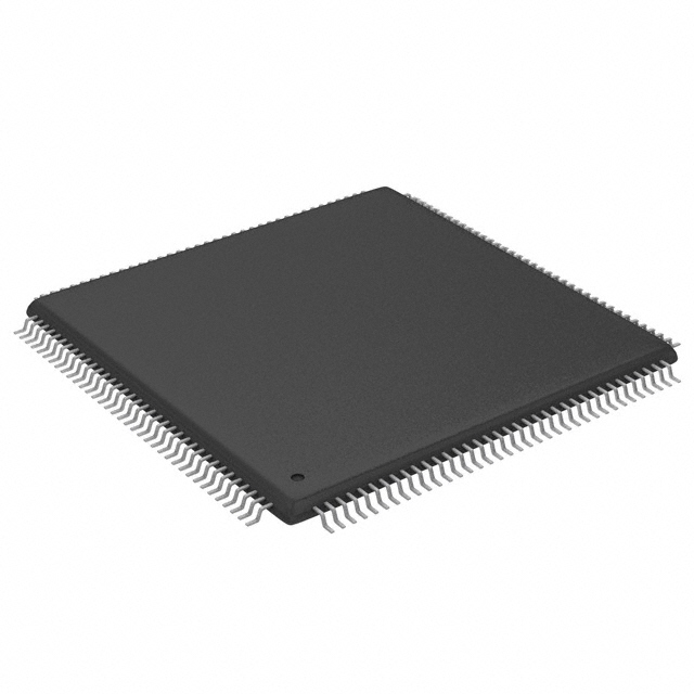

XC6SLX9-2TQG144I
Need wholesale pricing? Send RFQ now for the best rates and immediate response.
XC6SLX9-2TQG144I Description
XC6SLX9-2TQG144I Overview
The XC6SLX9-2TQG144I is a high-performance Field Programmable Gate Array (FPGA) manufactured by AMD, designed for a wide range of applications requiring versatile and efficient programmable logic solutions. This IC FPGA features 102 I/Os and is housed in a 144-pin TQFP package, making it suitable for surface-mount applications. It operates within a supply voltage range of 1.14V to 1.26V and is REACH unaffected and ROHS3 compliant, ensuring it meets stringent environmental and safety standards.
XC6SLX9-2TQG144I Features
- Total RAM Bits: 589,824 bits, providing substantial memory capacity for complex computations and data storage.
- Number of LABs/CLBs: 715 Logic Array Blocks/Configurable Logic Blocks, enabling the implementation of intricate logic functions.
- Number of Logic Elements/Cells: 9,152, offering extensive programmable logic resources.
- I/O Count: 102 I/O pins, supporting a wide array of peripheral connections and interfacing options.
- Package Type: 144TQFP, ideal for surface-mount technology (SMT) and compact board designs.
- Moisture Sensitivity Level (MSL): Level 3 (168 hours), ensuring reliability in various environmental conditions.
- ECCN: EAR99, indicating compliance with export regulations.
XC6SLX9-2TQG144I Applications
The XC6SLX9-2TQG144I is well-suited for a variety of applications across multiple industries, including:
- Telecommunications: For baseband processing, signal routing, and protocol conversion.
- Industrial Control: In automation systems, motor control, and real-time data processing.
- Consumer Electronics: In high-definition video processing, digital signal processing, and embedded systems.
- Automotive: For advanced driver assistance systems (ADAS), infotainment systems, and electronic control units (ECUs).
- Medical Devices: In diagnostic imaging, patient monitoring systems, and medical instrumentation.
XC6SLX9-2TQG144I Development Tools
AMD provides a comprehensive suite of development tools to support the XC6SLX9-2TQG144I, including:
- Integrated Development Environment (IDE): A user-friendly platform for designing, simulating, and debugging FPGA applications.
- IP Cores: A library of pre-designed intellectual property cores for common functions such as memory controllers, communication interfaces, and arithmetic operations.
- Reference Designs: Sample projects and documentation to help developers quickly get started and accelerate the development process.
- Evaluation Kits: Hardware platforms for testing and prototyping FPGA designs, ensuring compatibility and performance in real-world applications.
XC6SLX9-2TQG144I Advantages
- High Logic Density: The large number of logic elements and configurable logic blocks allows for the implementation of complex systems-on-chip (SoC) and multi-functional designs.
- Versatile I/O Options: With 102 I/O pins, the XC6SLX9-2TQG144I can interface with a wide variety of peripherals and communication protocols, enhancing its flexibility.
- Energy Efficiency: Operating within a low voltage range of 1.14V to 1.26V, this FPGA offers power-efficient solutions, making it suitable for battery-powered and energy-sensitive applications.
- Environmental Compliance: Being REACH unaffected and ROHS3 compliant, the XC6SLX9-2TQG144I meets global environmental regulations, ensuring its suitability for worldwide markets.
- Reliability: The MSL 3 (168 hours) rating ensures the FPGA's reliability in various environmental conditions, reducing the risk of moisture-related failures.
Conclusion of XC6SLX9-2TQG144I
The XC6SLX9-2TQG144I is a robust and versatile FPGA that offers a high density of logic elements, substantial RAM capacity, and extensive I/O capabilities. Its low power consumption, environmental compliance, and reliable performance make it an ideal choice for a wide range of applications in telecommunications, industrial control, consumer electronics, automotive, and medical devices. With AMD's comprehensive development tools and support, designers can efficiently develop and deploy advanced FPGA-based solutions, leveraging the XC6SLX9-2TQG144I's unique features and advantages to meet their specific requirements.
Tech Specifications
XC6SLX9-2TQG144I Documents
Download datasheets and manufacturer documentation for XC6SLX9-2TQG144I

