


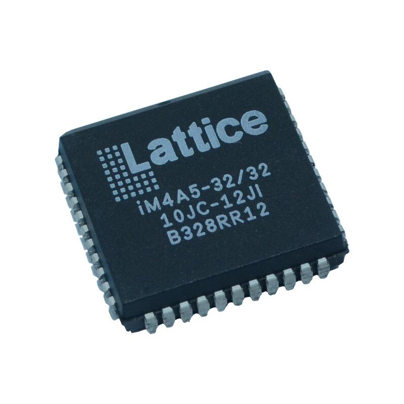
Lattice Semiconductor
ORSO82G5-2FN680I1
FPGAs (Field Programmable Gate Array)
ORSO82G5-2FN680I1
2-ORSO82G5-2FN680I1
FPGA - Field Programmable Gate Array 10368 LUT 372 I/O
In Stock : Please Submit RFQ TO US
Need wholesale pricing? Send RFQ now for the best rates and immediate response.
QUICK RFQ
ADD TO RFQ LIST
ORSO82G5-2FN680I1 Description
Tech Specifications
Mounting Style
SMD/SMT
Embedded Block RAM - EBR
111 Kbit
Package / Case
fpBGA-680
Number of Logic Blocks
1296
Operating Supply Voltage
1.425 V to 1.575 V, 3 V to 3.6 V
Number of I/Os
372
Number of Gates
333 K to 643 K
Maximum Operating Frequency
168 MHz
Maximum Operating Temperature
+ 125 C
Minimum Operating Temperature
- 40℃
Factory Pack Quantity
24
ORSO82G5-2FN680I1 Documents
Download datasheets and manufacturer documentation for ORSO82G5-2FN680I1
Related Parts
XC9572-7PCG84I
AMD
XCR5128-7TQ128I
AMD
QL80FC-APQ208C
QuickLogic
AX500-1FG676M
Actel
XC95108-VQ100
AMD
A54SX32A-2BGG329I
Microsemi
XC5202-3PQ100I
AMD
EX64-CS49
Actel
A42MX16-2VQG100
Microsemi
XCV1000E-8FG680I
AMD
A42MX24-2PQG160I
Microsemi
XC5206-3TQ144I
AMD
XC4085XL-BG560
AMD
Shopping Guide
Payment Methods
Payment Methods include Prepayment TT (bank transfer), Western Union, and PayPal. Customers are responsible for shipping costs, bank charges, customs duties and taxes.
Shipping Rate
Shipments are made once a day around 5pm, excluding Sundays. Once shipped, the estimated delivery time is usually 5-7 business days, depending on the courier you choose.
Delivery Methods
Provide DHL, FedEx, UPS, EMS, SF Express and Registered Airmail International Delivery Service
Follow Us
Please find more information about us from below social media and interact with us!
Contact With Us
TOOLS
payment
Transportation
Trademark
All Rights Reserved © 2025 AMPHEO PTY LTD