


Lattice Semiconductor
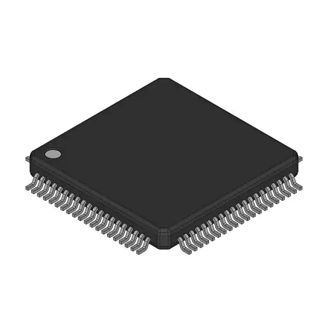
OR3LP26BBM680-DB
FPGAs (Field Programmable Gate Array)
OR3LP26BBM680-DB
2-OR3LP26BBM680-DB
FPGA - Field Programmable Gate Array FPSC PCI INTERFACE
In Stock : Please Submit RFQ TO US
Need wholesale pricing? Send RFQ now for the best rates and immediate response.
QUICK RFQ
ADD TO RFQ LIST
OR3LP26BBM680-DB Description
Tech Specifications
Mounting Style
SMD/SMT
Package / Case
PBGAM-680
Number of Logic Blocks
1024
Operating Supply Voltage
5 V
Packaging
Tube
Number of Gates
120 K
Maximum Operating Temperature
+ 70 C
Minimum Operating Temperature
0 C
Factory Pack Quantity
120
OR3LP26BBM680-DB Documents
Download datasheets and manufacturer documentation for OR3LP26BBM680-DB
Related Parts
MPF100TL-FCSG325I
Microsemi
XCS40XL-4C-BG256
AMD
XCR3128XL-VQ100
AMD
MPF300TL-FCG784I
Microsemi
A3PN060-Z1VQG100I
Microsemi
XCR3128-10TQ128C
AMD
XCR5064-10PC
AMD
XC9572XL-5VGQ64C
AMD
A1280A-PL84C
Actel
XCDAISY-CN1144
AMD
A1010B-1PQG100C
Microsemi
APA075-FTQG144P
Actel
A40MX04-PL68
Microsemi
QL3012-4PF144C
QuickLogic
M2S060-FCSG325
Microsemi
AGL400V5-FGG144
Microsemi
Shopping Guide
Payment Methods
Payment Methods include Prepayment TT (bank transfer), Western Union, and PayPal. Customers are responsible for shipping costs, bank charges, customs duties and taxes.
Shipping Rate
Shipments are made once a day around 5pm, excluding Sundays. Once shipped, the estimated delivery time is usually 5-7 business days, depending on the courier you choose.
Delivery Methods
Provide DHL, FedEx, UPS, EMS, SF Express and Registered Airmail International Delivery Service
Follow Us
Please find more information about us from below social media and interact with us!
Contact With Us
TOOLS
payment
Transportation
Trademark
All Rights Reserved © 2025 AMPHEO PTY LTD