


Lattice Semiconductor
OR2C06A3T100I-DB
FPGAs (Field Programmable Gate Array)
OR2C06A3T100I-DB
2-OR2C06A3T100I-DB
FPGA - Field Programmable Gate Array 576 LUT 192 I/O
In Stock : Please Submit RFQ TO US
Need wholesale pricing? Send RFQ now for the best rates and immediate response.
QUICK RFQ
ADD TO RFQ LIST
OR2C06A3T100I-DB Description
Tech Specifications
Mounting Style
SMD/SMT
Package / Case
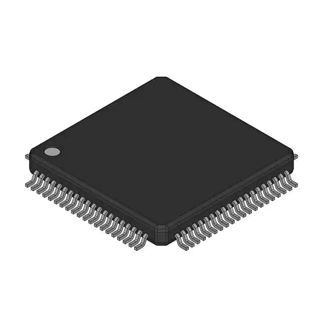
TQFP-100
Number of Logic Blocks
576
Operating Supply Voltage
3.3 V
Number of I/Os
192
Number of Gates
15.9 K
Maximum Operating Frequency
200 MHz
Maximum Operating Temperature
+ 85℃
Minimum Operating Temperature
- 40℃
Factory Pack Quantity
90
OR2C06A3T100I-DB Documents
Download datasheets and manufacturer documentation for OR2C06A3T100I-DB
Related Parts
EPF10K50SQC208-3N
Altera
EP1S60F1020I6N
Intel
A3PN030-ZQNG48
Microchip Technology
5SGXMA9K3H40I3N
Intel
EP20K200EQC208-1
Intel
5AGXBB3D4F40I5N
Intel
EP2AGZ300HF40I4N
Intel
A40MX04-PLG44M
Microchip Technology
LFE2M20SE-5FN256I
Lattice Semiconductor Corporation
5SGXEA7K2F35I2N
Intel
A42MX16-1PLG84M
Microchip Technology
EPCS64SI16N
Intel
EPF10K50SQC208-2
Altera
XC3S500E-4CP132I
AMD
AGL600V5-FG256
Microchip Technology
Shopping Guide
Payment Methods
Payment Methods include Prepayment TT (bank transfer), Western Union, and PayPal. Customers are responsible for shipping costs, bank charges, customs duties and taxes.
Shipping Rate
Shipments are made once a day around 5pm, excluding Sundays. Once shipped, the estimated delivery time is usually 5-7 business days, depending on the courier you choose.
Delivery Methods
Provide DHL, FedEx, UPS, EMS, SF Express and Registered Airmail International Delivery Service
Follow Us
Please find more information about us from below social media and interact with us!
Contact With Us
TOOLS
payment
Transportation
Trademark
All Rights Reserved © 2025 AMPHEO PTY LTD