


Lattice Semiconductor
OR2C04A4M84-D
FPGAs (Field Programmable Gate Array)
OR2C04A4M84-D
2-OR2C04A4M84-D

FPGA - Field Programmable Gate Array 400 LUT 160 I/O
In Stock : Please Submit RFQ TO US
Need wholesale pricing? Send RFQ now for the best rates and immediate response.
QUICK RFQ
ADD TO RFQ LIST
OR2C04A4M84-D Description
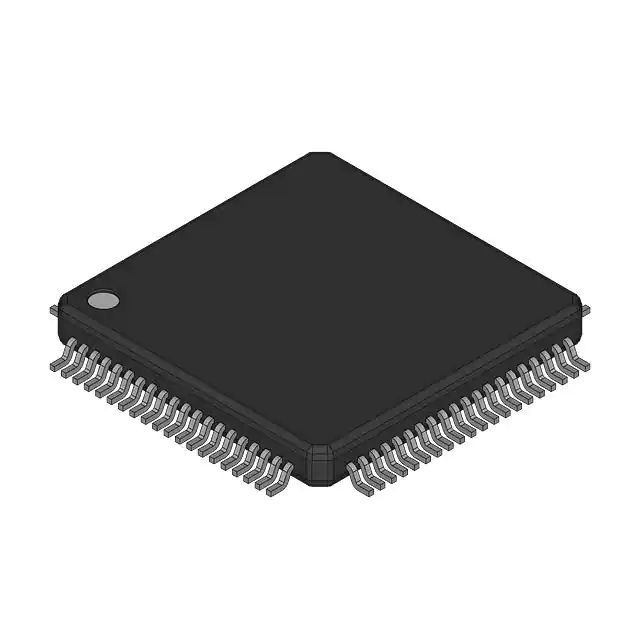
ORCA™2 Field Programmable Gate Array (FPGA) IC 160 6400 400 84-LCC (J-Lead)
Tech Specifications
Operating Temperature
0°C ~ 70°C (TJ)
Total RAM Bits
6400
ECCN
EAR99
Number of I/O
160
Mounting Type
Surface Mount
Product Status
Active
Supplier Device Package
84-PLCC (29.08x29.08)
Series
ORCA™2
Package / Case
84-LCC (J-Lead)
Voltage - Supply
3V ~ 3.6V
REACH Status
Vendor Undefined
Mfr
Lattice Semiconductor Corporation
Number of Gates
11000
HTSUS
8542.39.0001
Package
Bulk
Number of Logic Elements/Cells
400
RoHS Status
RoHS non-compliant
Moisture Sensitivity Level (MSL)
3 (168 Hours)
OR2C04A4M84-D Documents
Download datasheets and manufacturer documentation for OR2C04A4M84-D
Related Parts
XC5202-4PCG84C
AMD
XCF04SVOG20I
AMD
A3P1000-4PQ208M
Actel
RTAX2000SL-1LG1152V
Actel
XCV800-5PQG240C
AMD
MPF300T-FCG1152I
Microsemi
XC4036EX-2PQ240C
AMD
XC4013XL-PQ240
AMD
RTSX72SU-CG624E
Actel
XCV100-5PQG240I
AMD
QL8X12B-0PL68I
QuickLogic
M2S060-VFG400I
Microsemi
QL3012-2PF144
QuickLogic
Shopping Guide
Payment Methods
Payment Methods include Prepayment TT (bank transfer), Western Union, and PayPal. Customers are responsible for shipping costs, bank charges, customs duties and taxes.
Shipping Rate
Shipments are made once a day around 5pm, excluding Sundays. Once shipped, the estimated delivery time is usually 5-7 business days, depending on the courier you choose.
Delivery Methods
Provide DHL, FedEx, UPS, EMS, SF Express and Registered Airmail International Delivery Service
Follow Us
Please find more information about us from below social media and interact with us!
Contact With Us
TOOLS
payment
Transportation
Trademark
All Rights Reserved © 2025 AMPHEO PTY LTD