


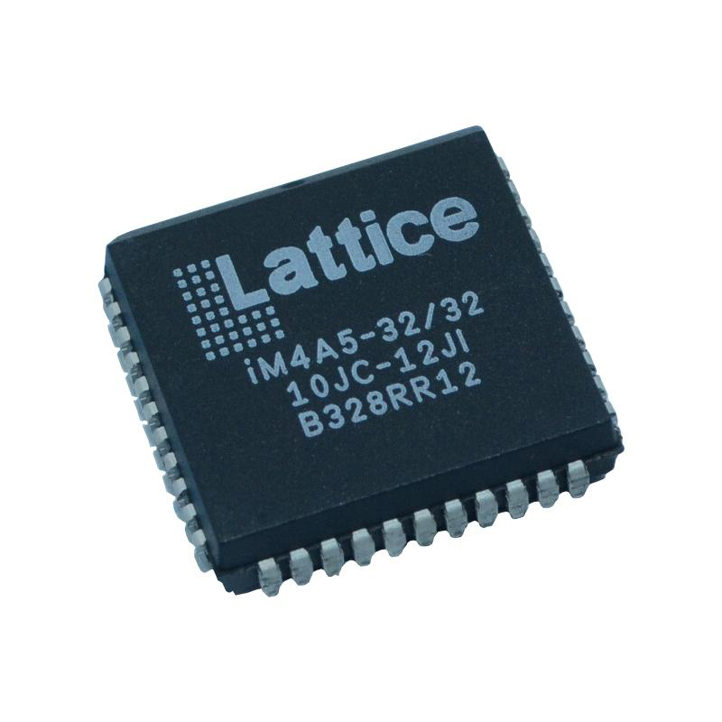
Lattice Semiconductor
LFSC3GA40E-6FCN1152I
FPGAs (Field Programmable Gate Array)
LFSC3GA40E-6FCN1152I
2-LFSC3GA40E-6FCN1152I
FPGA LatticeSC Family 40000 Cells 90nm Technology 1.2V 1152-Pin CFCBGA
In Stock : Please Submit RFQ TO US
Need wholesale pricing? Send RFQ now for the best rates and immediate response.
QUICK RFQ
ADD TO RFQ LIST
Tech Specifications
Mounting Style
SMD/SMT
Package / Case
CFCBGA-1152
Number of Logic Blocks
216
Operating Supply Voltage
1.2 V
Packaging
Tray
Number of I/Os
604
Number of Gates
40 K
Maximum Operating Temperature
+ 105 C
Minimum Operating Temperature
- 40℃
Factory Pack Quantity
72
LFSC3GA40E-6FCN1152I Documents
Download datasheets and manufacturer documentation for LFSC3GA40E-6FCN1152I
Related Parts
M2S025T-1FCSG325
Microsemi
A54SX32A-FGG144M
Microsemi
XC3030ATM-7CPC84
AMD
M1A3P600-PQ208I
Microsemi
XC17V16PC44I
AMD
OR2T15A7BA256-DB
Lattice Semiconductor
M2GL150TS-FCS536I
Microsemi
A42MX16-3PQG208
Microsemi
XC2VP7-7FGG256I
AMD
A40MX04-2PQG100
Microsemi
M1A3P1000-2PQ208
Microsemi
APA075-FGG144I
Microsemi
OR2C12A4BA352-DB
Lattice Semiconductor
XC3064-125PC84I
AMD
XC3164A-5PC84C
AMD
M2GL060TS-FG676
Microsemi
M2S060-FG484I
Microsemi
Shopping Guide
Payment Methods
Payment Methods include Prepayment TT (bank transfer), Western Union, and PayPal. Customers are responsible for shipping costs, bank charges, customs duties and taxes.
Shipping Rate
Shipments are made once a day around 5pm, excluding Sundays. Once shipped, the estimated delivery time is usually 5-7 business days, depending on the courier you choose.
Delivery Methods
Provide DHL, FedEx, UPS, EMS, SF Express and Registered Airmail International Delivery Service
Follow Us
Please find more information about us from below social media and interact with us!
Contact With Us
TOOLS
payment
Transportation
Trademark
All Rights Reserved © 2025 AMPHEO PTY LTD