


Lattice Semiconductor
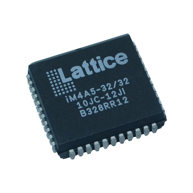
ISPPAC-CLK5610V-0
FPGAs (Field Programmable Gate Array)
ISPPAC-CLK5610V-0
2-ISPPAC-CLK5610V-0
In-System Programmable, Enhanced Zero-Delay Clock Generator with Universal Fan-Out Buffer
In Stock : Please Submit RFQ TO US
Need wholesale pricing? Send RFQ now for the best rates and immediate response.
QUICK RFQ
ADD TO RFQ LIST
ISPPAC-CLK5610V-0 Description
In-System Programmable, Enhanced Zero-Delay Clock Generator with Universal Fan-Out Buffer
Tech Specifications
Operating Temperature
-40°C ~ 85°C
Ratio - Input:Output
1:10
Differential - Input:Output
Yes/Yes
Mounting Type
Surface Mount
PLL
Yes with Bypass
Series
ispClock
Input
HSTL, LVCMOS, LVDS, LVPECL, LVTTL, SSTL
Voltage - Supply
3V ~ 3.6V
Output
EHSTL, HSTL, LVCMOS, LVDS, LVPECL, LVTTL, SSTL
Packaging
Tray
Part Status
Obsolete
Divider/Multiplier
Yes/No
Number of Circuits
1
Frequency - Max
400MHz
ISPPAC-CLK5610V-0 Documents
Download datasheets and manufacturer documentation for ISPPAC-CLK5610V-0
Related Parts
A3PE600-1FG484
Microsemi
QL8X12B-XPF100C
QuickLogic
A54SX08A-FTQ100
Microsemi
A54SX16-TQG176
Microsemi
XCS30-3VQ100I
AMD
EX64-FCS128
Actel
A42MX16-1PQG208
Microsemi
RTSX32SU-CQ208E
Actel
QL2009-2PQ208C
QuickLogic
A42MX24-PL84
Actel
A2F060M3E-CS288I
Actel
M1AGL600V2-CSG281I
Microsemi
M7A3P1000-1FGG256
Microsemi
XC5202-6VQ64C
AMD
QL7100-4PQ208I
QuickLogic
Shopping Guide
Payment Methods
Payment Methods include Prepayment TT (bank transfer), Western Union, and PayPal. Customers are responsible for shipping costs, bank charges, customs duties and taxes.
Shipping Rate
Shipments are made once a day around 5pm, excluding Sundays. Once shipped, the estimated delivery time is usually 5-7 business days, depending on the courier you choose.
Delivery Methods
Provide DHL, FedEx, UPS, EMS, SF Express and Registered Airmail International Delivery Service
Follow Us
Please find more information about us from below social media and interact with us!
Contact With Us
TOOLS
payment
Transportation
Trademark
All Rights Reserved © 2025 AMPHEO PTY LTD